HEF ?
In the microcontroller, the presence of EEPROM is very useful for saving user settings, calibration data and the like. What is written in EEPROM continues even if the chip is not
alimentato.
In the newer PIC, Microchip has replaced EEPROM with HEF, which stands for High Endurance
Flash.
However, HEF is not the same as EEPROM and the only specific documentation on High Endurance Flash (HEF) is the AN1673
and what is written on the data sheets of the various components.
Also because there is still some confusion due to the fact that in some specific chip indicates EEPROM, and then it comes to
HEF e non solo.
Data shows that the HEF area, which is the last leases (typ. 128 ) of Flash, it has a minimum guaranteed lifetime of 100K write cycles, compared to the rest of the 10K Flash. This brings the durability (endurance) of the HEF to be comparable with those of the
EEPROM.
The essential difference is that HEF is part of the program memory FLASH: it is therefore to write and read data from an area of
Flash, which, in Enhanced Midrange and Midrange, it is the same bus width instruction, or 14
bit.
Because the data bus is 8-bit, data sheets affirm that only the lower 8 bits of the leases HEF are validly used.
From this it should be stated that the breaking locations are composed of Flash program memory able to contain 14 bits (as well as the rest of the Flash memory), but of which the 8 bits LSB are HEF Flash and the 6-bit MSB are flash normal.
It follows that every write will have to act in HEF flash on the low 8 bits, discarding the 6-bit
alti.
In any case, HEF is on Flash and differ from module to the EEPROM data in two
ways. In HEF:
- The data must be deleted manually before writing and this can only be done in blocks (called
row) of a fixed size (typically 16 or 32 locations)
- Writing the Flash it stall the CPU for a few milliseconds (param. D123 , typically 2-2.5ms)
By contrast, in an EEPROM data can be written byte by byte and there is no stall in the CPU during writing, even if, for reasons of constructional simplicity, most applications will include a delay loop to ensure that the writing is completed before the next
passo.
These differences imply that there are differences in the processing of data in HEF than previously seen for EEPROM and the need for a proper understanding of the mechanisms when replacing HEF in some
EEPROM.
See now some details.
Making all the following examples we refer to Enhanced Midrange group 16F150x, but this applies equally to the other chips with HEF, with the obligation to verify the position in the memory map of the HEF , its extension
and line width, parameters that can vary depending on the chip.
Operations in HEF.
HEF is Flash, and then the operations of reading and writing employ the same procedures that are employed for the Flash "normal".
The only difference is that, of the 14 bytes read, only the first 8 (LSB) to be considered, while
remaining 6 are discarded.
We see in detail the different operations.
Read the HEF.
Regarding the reading of data in the HEF, there are no limitations in size, nor much less is required a stall of the MPU.
The essential problem is that the reading of the flash is not the same thing as the reading of the RAM, as it requires, similarly to what accesses to the EEPROM, a specific procedure, with the 'use of dedicated registers.
For Enhanced Midrange it registers PMADRL
and PMADRH for address and registers PMADRL
and PMADRH for the data. Also, it comes in the register
PMCON1.
Important to consider that these chips typically have the RAM area divided into as many as 32 banks and that the records management operations in Flash are typically found in bank 3, which requires the
use of the switch banks.
If the Enhanced Midrange simplify this task with the opcode bsr,
the use of the classic BANKSELL it is the most practical solution, since it is valid for any family of PIC
 |
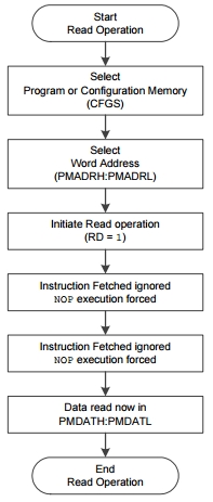
The operation is not complex and can be divided into three phases:
-
place in the records and PMADRL
and PMADRH the desired address
-
select the register reading mode of area Flash
-
retrieve the data in the registers and PMDATL
and PMDATH
The address may be any one to 'internal' s area HEF.
If the use of a pair of registers for the address is evident, it becomes less immediate need of a pair of registers for read data. However, if we remember how the Flash program memory is a 14-bit, it follows that the use of these data as providing for the division into a low byte 8 bits and in one upper 6 bits.
In fact, we see in the routine below, similar to that of the reading of a data in a general location of the Flash, as the high byte is discarded, also because, as stated initially, is not HEF and therefore unsuitable to support with a security number high of write
cycles.
Observe the need to introduce two nop
once started the read operation: this extra time is necessary since the processor has two fetch of instruction which will ignore; inserting two nop resolves the
problem.
|
Here's an example of how you can turn it into instructions that will ignore; inserting two nop resolves the
problem:
; Legge 1
byte dall'indirizzo HEF_ADDR
Read_HEF
BANKSEL PMADRL ; Select Bank for PMCON registers
movlw low(HEF_ADDR) ; Load initial address
movwf PMADRL
movlw high(HEF_ADDR)
movwf PMADRH
bcf
PMCON1,CFGS ; select flash Space
bsf PMCON1,RD
; Initiate read
nop
nop
; get only LSB - 8 bit HEF
movf PMDATL,W
; Get LSB of word
return |
The transfer of the data from the flash cell to the data bus is immediate, but 's operation to get to this figure, as we see, requires numerous instructions. It follows that, needing to read data in HEF the most sensible procedure is to perform, for example at the beginning of the program, transfers the contents of block and copy it in one of the RAM data available, from which the data will be accessible immediately.
The following routine uses the 'indirect addressing post indexed FSR0++
and the opcode movwi specific form the set of Enhanced Midrange to move a row to a HEF an area RAM data.
The address HEF_ADDR will be to start the line you want to copy.
; Copia 32 bytes
dall'indirizzo HEF_ADDR alla RAM all'indirizzzo hefdata
; Scarta MSB delle word
Read_HEF32:
BANKSEL PMADRL
; Select Bank for PMCON registers
movlw
low(HEF_ADDR) ; Load initial HEF address
movwf
PMADRL
movlw
high(HEF_ADDR)
movwf
PMADRH
movlw
LOW hefdata ; Load initial data address
movwf
FSR0L
movlw
HIGH hefdata
movwf
FSR0H
RdH_lp bcf
PMCON1,CFGS ; select flash Space
bsf
PMCON1,RD ; Initiate read
nop
nop
; get only LSB - 8 bit HEF
movf
PMDATL,W ; Get LSB of word
movwi
FSR0++ ; Store in user location
; i byte alti vengono scartati
;movf PMDATH,W
;movwf data_hi
movf
PMADRL,W ; Check lower bits of address
xorlw
0x1F ; Check if we're on the last of 32 addresses
andlw
0x1F
skpnz
goto
RdH_end
incf
PMADRL,f
bra
RdH_lp
RdH_end:
return |
HEF's address.
We mentioned that the HEF occupies the 'last part of Flash and therefore its starting address depends on the processor considered. Unfortunately the data sheets are obscure and confused on the subject, so very irritating.
Be sought with great patience as it serves to define the HEF area.
We find some of the information in the section and part which describes operations in Flash, but we may well be confronted with data sheets reluctant or completely unpacked.
For example, for the 10F320 data sheet DS40001585C-page 2 indicates a Flash Program Memory 512 words, which would amount to an area between 000 and 1FFh. Unfortunately the same document, on page 9 shows the TABLE 2.1:

which is clearly an error in the 'Address Range of both areas HEF, the Silicon Errata and Data Sheet Clarification DS80000529F not correct, let alone
"clarification".
It is not secondary, since the data sheet does not specify the size of the HEF, that we find clearly stated only in
the general
description of the chip , where they are declared 128 bytes.
Now, if the Flash 10F320 is 256, it begins at 00 and ends at FFh. If 128 are HEF, this takes up half of the Flash: starts at 80h and ends at FFh!
On the other hand, we have the 'indication "spot" that only the low byte is
HEF.
Need to go to the chapter on the Flash, page 91, to get to know that the line has a width of 16
words.
Quite similar to the situation of information for other chip; rather bleak for what should be a technical documentation of a complex
component.
Anyway, here are some of the features:
| PIC |
Flash |
Inizio HEF |
Dimensione |
Riga |
| 16F1507 |
2k |
0780h |
128 |
32 |
| 16F1508 |
4k |
0F80h |
128 |
32 |
| 16F1509 |
8k |
1F80h |
128 |
32 |
| 16F1516/7 |
8k |
1F80h |
128 |
32 |
| 16F1518/9 |
16k |
3F80h |
128 |
32 |
| 10F320 |
256 |
80h |
128 |
16 |
| 10F322 |
512 |
180h |
128 |
16 |
These elements will be used for definitions in the source. For example, to load a pre row:
; HEF memory preload
#ifdef __16F1508
HEFDATA CODE 0F80h
#endif
#ifdef __16F1509
HEFDATA CODE 1F80h
#endif
#ifdef __16F1507
HEFDATA CODE 0780h
#endif
DA 60h, 0, 99h, 9, 40h, 03h, 0, 0 ;8 bytes
DA
"MICROCONTROLLER.IT@ 2015"
;24 bytes - tot 32 bytes |
MCU stall.
In contrast to the behavior of an EEPROM, the MCU is not able to retrieve new instructions from the Flash during a cycle of self-writing, and is, therefore, stalled until the 'write operation (or deletion) is not It ended: we must be quite clear that the writing in Flash involves the fact that Flash is the same 'area that contains the codes of the instructions: If we are writing in, we can not simultaneously read opcodes ....
This means that no other action can be performed during a cancellation or writing, or you can respond to interrupt, which is to be disabled.
When writing, the code execution resumes automatically. The designer must, therefore, take into
account of the additional jitter introduced or blocking momentary application during updates of non-volatile
memory.
It should be noted that the duration of the stall is independent of the amount of data written in a row, operation performed in a single action.
The problem of the stalemate of the MCU, despite what you may fear, usually is not at a critical event. Simply consider the presence of this time and perform upgrades Flash in moments of the program in which it does not cause problems. In practice, it is a limited time (max. 2.5ms), is not perceptible by
user (for example, does not disturb the multiplex even of a group of seven-segment display, even if suspending
the interrupt). Only in the event that the management of interrupt is critical, it is necessary to define with precision the time of the transactions on the HEF, for example
to switch on and switch off.
Erase a row.
If there are no limitations on the data read from the HEF, when you write or delete a given must ensure its 'correct alignment in the matrix, which is all' inside of a block, or
row.
This means that you can not write (delete) a single byte, but it is necessary to rewrite or delete the 'entire line.
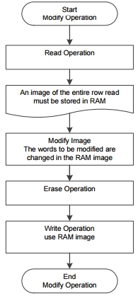
Therefore, a refresh operation of the HEF, even for a single element, should consider the following
actions:
- copy in RAM of the row that contains the data
- Changes to the data in RAM
- erase the row on HEF
- Writing the row
To be noted that the cancellation is required, by itself, only for the bits that are located at level 0: the Flash "canceled" has bits set to level 1. However, if even one bit of the row contains a 0, the cancellation concerns' entire line.
Fortunately we will see immediately that Microchip has implemented a very efficient system for the
erasing or writing of the line is carried out in a single operation.
 |
Here is the flow chart of the operations necessary for the cancellation of an entire
row.
First, if the interrupt is enabled, you must disable it.
As for reading, it leans to the special registers and PMADRL/PMADRH which, remember, are not in
Bank 0.
The cancellation is starting from 'address of beginning of the line, but, in fact, just provide an address line and the cancellation is made for the entire
row.
The register must be initialized by selecting the memory bit CFGS.
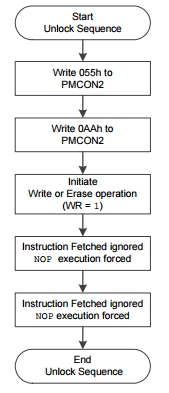
As for the EEPROM, you must be a "key" to access the operations of erase and write, and this is constituted by a precise sequence of
instructions.
After programming the bits FREE and WREN to enable cancellation, occorreà write a "key" AAh and 55h.
At this point you start deleting and MPU stalls for 2-2.5ms. During this time the processor is the I / O are
frozen.
Out of the stall time, the program will start automatically dall'opcode next.
It will take time to disable writing with bit WREN and rehabilitate, if requested, the
'interrupt.
As can be seen, a procedure quite similar to that used for the
EEPROM.
|
and now the assembly:
; Cancella una riga di HEF (32 word)
Erase_HEF
bcf INTCON,GIE
; Disable int
BANKSEL PMADRL
movlw low(HEF_ADDR) ; lower
address
movwf PMADRL
movlw high(HEF_ADDR) ; upper
address
movwf PMADRH
bcf PMCON1,CFGS ; Not configuration space
bsf PMCON1,FREE ; Specify an erase operation
bsf PMCON1,WREN ; Enable writes
movlw 055h
; Start erase sequence
movwf PMCON2
movlw 0AAh
movwf PMCON2
bsf PMCON1,WR
; Set WR bit to begin erase
nop
nop
; The processor stalls until the erase process is complete
; after erase processor continues with 3rd instruction
bcf PMCON1,WREN ; Disable writes
bsf INTCON,GIE
; Enable interrupts
return
|
We observe that they do not serve "data" for the cancellation; delete a location simply means bringing the electric level of the bits to 1. Consequently a lease to remove 14-bit will 3FFh.
 |
For clarity, this structure is the "key":
It uses a specific SFR, PMCON2, which must be written in the order indicated, the keys AAh and 55h.
Remenber: 55h= 01010101 bin and AAh=10101010 bin.
To observe the need of the two nop already seen for reading.
If you are not using this algorithm, you can not erase or write in Flash.
Its necessity is evident, since the Flash contains the firmware, which should not risk being damaged by random events, but which can be modified only following a voluntary action of the program. |
Writing a row.
ASimilarly, the cancellation, writing requires a "key", but, this time, also data.
Having to write an entire line at a time, you need a system to prevent a repeat of 16 or 32 stalls to writing each byte. The mechanism implemented by the manufacturer is that of a buffer, as wide as the line, which is written in Flash in a single action, reducing the stall to the already seen 2-2.5ms.
Obviously, the buffer must be loaded with the 14-bit word and this requires a number of instructions here is the flowchart recommended by the data sheet.
We observe that in the writing of the latches do not need any delay.
In instructions. We copy a line of 32 bytes from the RAM to the
HEF.
The Flash is composed of two "bytes", an 8-bit and a 6-bit. We are concerned, since the HEF, only the 8bit and discard the 6, charging it with a dummy value.
; Copia 32 bytes da RAM dall' indirizzo hefdata all'indirizzo
; HEF_ADDR della HEF
; Dati immagazzinati in formato little endian
; L'MSB delle word è il valore dummy 3Fh
Write_HEF
bcf
INTCON,GIE ; Disable ints
BANKSEL PMADRH
; Bank 3
movlw low(HEF_ADDR)
; Load initial address
movwf PMADRH
movlw high(HEF_ADDR)
movwf PMADRL
movlw LOW hefdata
; Load initial data address
movwf FSR0L
movlw HIGH hefdata
movwf FSR0H
bcf
PMCON1,CFGS ; Not configuration space
bsf
PMCON1,WREN ; Enable writes
bsf
PMCON1,LWLO ; Only Load Write Latches
WHlp moviw FSR0++
; Load first data byte into lower
movwf PMDATL
;moviw FSR0++ ; discard second data byte
movlw 3Fh
; and use dummy value for MSB
movwf PMDATH
movf
PMADRL,W ; Check if lower
address
xorlw 0x1F
andlw 0x1F
skpnz
; Exit if last of 32 words
bra
WHstart ;
otherwise re loop
movlw 055h
; write sequence
movwf PMCON2
movlw 0AAh
movwf PMCON2
bsf
PMCON1,WR ; Set WR bit to begin write
nop
nop
incf PMADRL,F
; latches Increment address
bra
WHlp ; Write next latches
WHstart
bcf
PMCON1,LWLO ; memory write
movlw 055h
; write sequence
movwf PMCON2
movlw 0AAh
movwf PMCON2
bsf
PMCON1,WR ; Set WR bit to begin write
nop
; all latches simultaneously
nop
; to program memory.
; the processor stalls until the self-write process complete. ; After write processor continues
bcf
PMCON1,WREN ; Disable writes
bsf
INTCON,GIE ; Enable interrupts
return
|
We observe how the 'use indirect addressing post increased and the opcode moviw facilitate the operation.
The MSB (6 bits HEF) is loaded with a value that has all the bits to 1 and prevents a useful in
writing.
Modify dat in HEF.
 |
Changing the content of the HEF is achievable simply by organizing what has been
said.
We must always start from the basic concept is that the
operation on a whole line, whether it is to change a single byte or more
bytes.
The content of the line has placed as an image in RAM: in appropriate areas can copy the contents of the line.
Changes will be made on this in RAM.
Then you will delete the line and rewrite it with the desired
content.
The operations of the data blocks are easily achievable with the 'use indirection and new
instructions. |
Here is an example of a macro for moving a certain number of bytes from RAM area to another.
; Copy n bytes da source a target
COPYMEM MACRO source, target, nbyte
local c_0
movlw nbyte
movwf temp
movlw low(source)
movwf FSR0L
movlw high(source)
movwf FSR0H
movlw low(target)
movwf FSR1L
movlw high(target)
movwf FSR1H
c_0 moviw FSR0++
movwi FSR1++
decfsz temp,f
bra
c_0
ENDM |
We observe the use of two pointers and indirect pair Operatin moviw - movwi.
Source and destination can be in any bank, given that, through the FSR we can reach any point of the RAM. The post increase reduces the number of instructions needed for the loop.
Verifiy.
 |
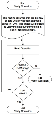
After a write, it may want to verify that the data has been successfully copied in
HEF.
The process is semplice.
Consideriamo as a reference data set that we copied from RAM buffers for writing Flash.
We read one by one the elements of the row just written, and we compare them with the copy in RAM. If there are differences, the writing is not successful and you have to take the appropriate
decisions.
If we have taken care to carry out various tasks such as subroutines or macros, their reuse is immediate and allows a significant savings of time and resources. |
And for the C compiler?
The AN1673
concerns the problem from the point of view of the C compiler, for which there is a specific library for writing the Flash..
|